ADF4350 PLL Phase-locked loop Rf Signal Source Frequency Synthesizer
ADF4350 PLL Phase-locked loop Rf Signal Source Frequency Synthesizer
In stock
-
All orders are dispatched the next 3 business days!
-
We will beat any price. We back all products with a 1 year guarantee.
Order in the next 0 hours 0 minutes to get it by /06/2026
Couldn't load pickup availability
Guaranteed Safe Checkout
Product Use:
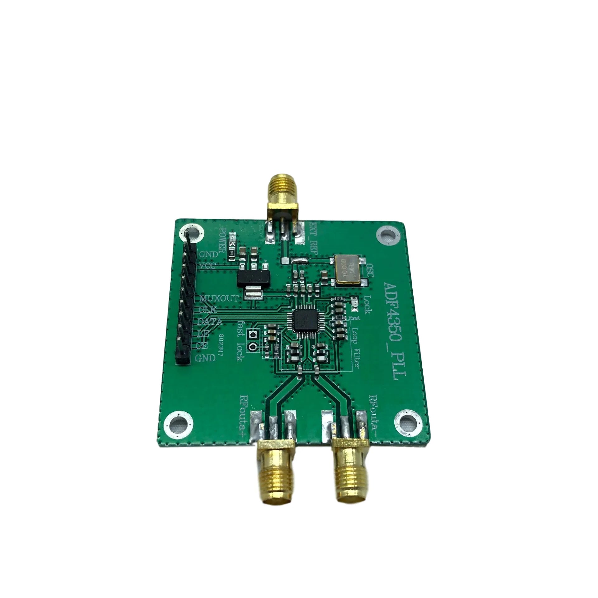
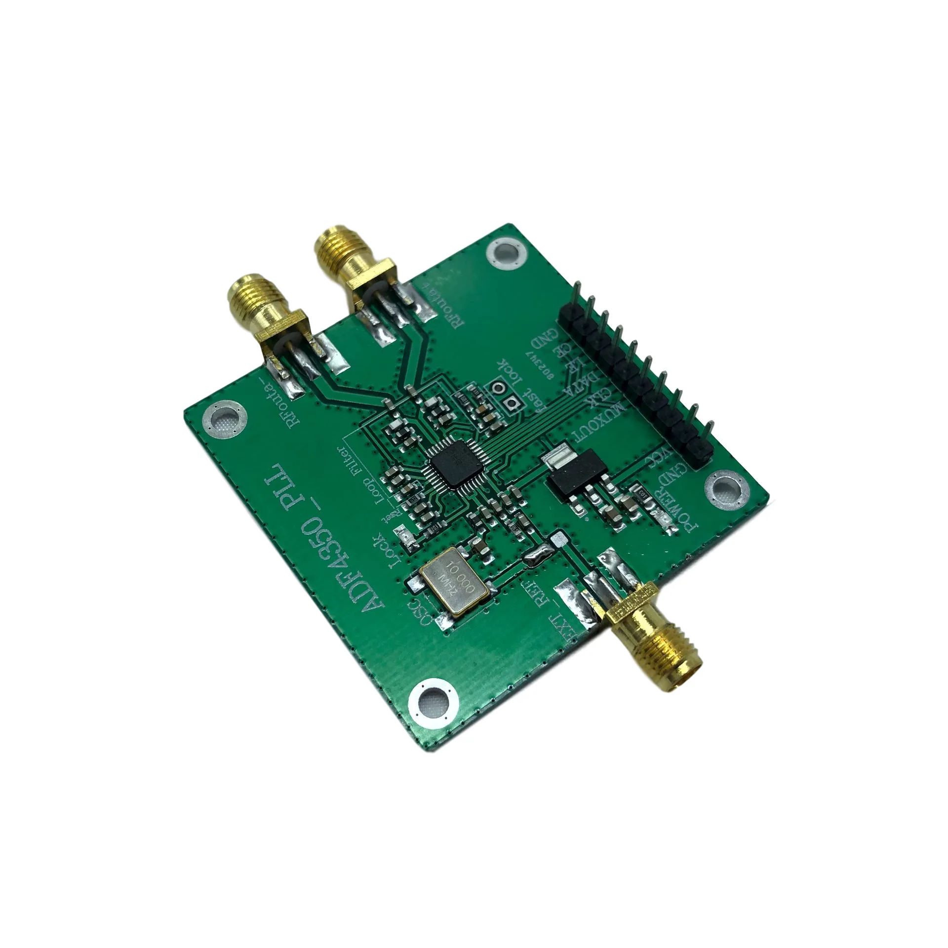
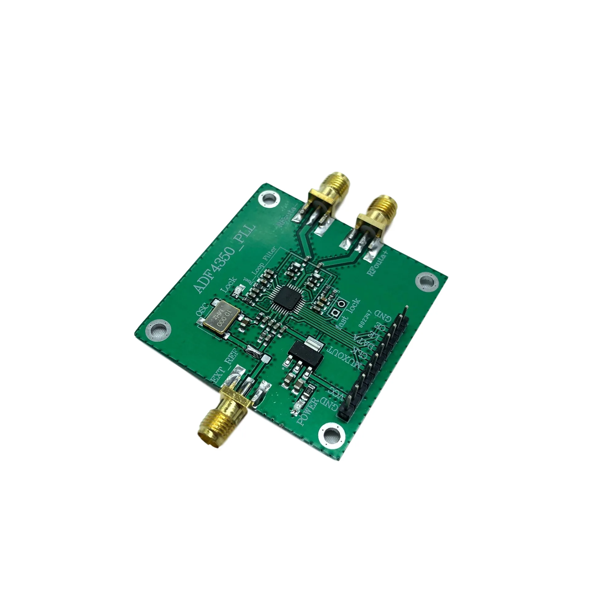
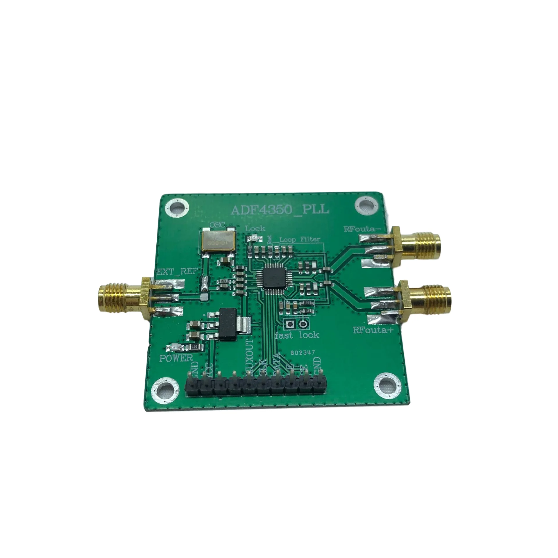
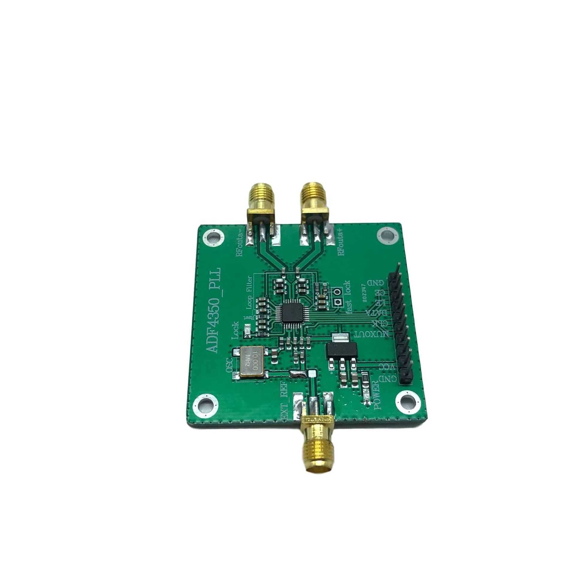
Adf4350/4351 Development Board Reference Official Circuit Principle Design, Output Frequency Range: 137m-4.4ghz
(ADF4350),35M-4.4G(ADF4351)
Technical Parameters:
1. Output Frequency Range:137MHz-4.4GHz(ADF4350)
35MHz--4.4GHz(ADF4351)
2. Power Supply Voltage: 4-9v (5vdc)
3. Output Signal: 2.2ghz--4.4GHz Sine Wave (Fundamental Wave)
137MHz -- 2.2GHz (Adf4350) Square Wave (Fundamental Frequency Division)
35mhz---2.2GHz (Adf4351) Square Wave (Fundamental Frequency Division)
4. Output Signal: Output Is Broadband, Signal Strength: 5dbm (Programmable Setting)
5. RF Connector: SMA Female Head
6. Control Interface: Three-Wire SPI
7. Reference Clock: 10.000MHz (Default), Which Can Be External through SMA Interface
8. Weight: 15G
Wiring Method:
This Module Can Be Connected by Using the Pins of the Lcd1602/Lcd12864 Module on the Single Chip Microcomputer (It Can Be Directly Plugged in Upside down), Which Is Convenient for Software Debugging and Has a Lock Indication (Lock) at the Same Time. The Pin Corresponds to the following:
LCD1602/LCD12864 ADF4350/ADF4351
1.GND------------------------- GND
2.VDD(5V)-------------------VCC
3.vo-------------------------- NC (Empty)
4.rs-------------------------- NC (Empty)
5.R/ W-------------------------MUXOUT
6.EN- ----------------------- CLK
7.DB0-------------------------DATA
8.DB1 ------------------------- LE
9.DB2-------------------------CE (10K Pull-up)
10.DB3-------------------------GND (No Connection)
Reference Clock:
The Default Reference Clock Signal Is a 10.000MHz Active Clock. You Can Also Use an External Reference Clock Signal. You Need to Modify the Soldering Iron Method by Using Tee Junction to Connect Ext_ref to an External Reference Signal.
RF Output:
For Convenience, the Default Is Broadband Output, and the Output Is Two Differential Signals. One Can Be Used for Output and the Other Can Be Used for Monitoring Output.

Description
Description
Product Use:
Adf4350/4351 Development Board Reference Official Circuit Principle Design, Output Frequency Range: 137m-4.4ghz
(ADF4350),35M-4.4G(ADF4351)
Technical Parameters:
1. Output Frequency Range:137MHz-4.4GHz(ADF4350)
35MHz--4.4GHz(ADF4351)
2. Power Supply Voltage: 4-9v (5vdc)
3. Output Signal: 2.2ghz--4.4GHz Sine Wave (Fundamental Wave)
137MHz -- 2.2GHz (Adf4350) Square Wave (Fundamental Frequency Division)
35mhz---2.2GHz (Adf4351) Square Wave (Fundamental Frequency Division)
4. Output Signal: Output Is Broadband, Signal Strength: 5dbm (Programmable Setting)
5. RF Connector: SMA Female Head
6. Control Interface: Three-Wire SPI
7. Reference Clock: 10.000MHz (Default), Which Can Be External through SMA Interface
8. Weight: 15G
Wiring Method:
This Module Can Be Connected by Using the Pins of the Lcd1602/Lcd12864 Module on the Single Chip Microcomputer (It Can Be Directly Plugged in Upside down), Which Is Convenient for Software Debugging and Has a Lock Indication (Lock) at the Same Time. The Pin Corresponds to the following:
LCD1602/LCD12864 ADF4350/ADF4351
1.GND------------------------- GND
2.VDD(5V)-------------------VCC
3.vo-------------------------- NC (Empty)
4.rs-------------------------- NC (Empty)
5.R/ W-------------------------MUXOUT
6.EN- ----------------------- CLK
7.DB0-------------------------DATA
8.DB1 ------------------------- LE
9.DB2-------------------------CE (10K Pull-up)
10.DB3-------------------------GND (No Connection)
Reference Clock:
The Default Reference Clock Signal Is a 10.000MHz Active Clock. You Can Also Use an External Reference Clock Signal. You Need to Modify the Soldering Iron Method by Using Tee Junction to Connect Ext_ref to an External Reference Signal.
RF Output:
For Convenience, the Default Is Broadband Output, and the Output Is Two Differential Signals. One Can Be Used for Output and the Other Can Be Used for Monitoring Output.
Item Specifics
Item Specifics